|
|
|
|
 |
|
Sapphire Wafer SPEC
|


|

 |
Sapphire Wafer SPEC
Sapphire Wafer 란?
Al2O3가 2300도 이상에서 단결정으로 성장된 결정체를 Sapphire라고 합니다.
Sapphire 특성
1. 저온 및 고온 안정성
- 극저온에서 초고온까지 상변태없이 매우 안정적이다.
2. 우수한 기계적 성질 (Knoop 2000), 경도가 Mohs9 로써 다이아몬드 다음으로 높다.산과 알카리에 상당히 강함.
3. 뛰어난 광학특성
-빛의 투과성이 가장 뛰어난 재료, Index of refraction : 1.769
4. 우수한 열전달 특성
- 세라믹 재료중에서 금속과 맞먹는 열전도도를 가짐
- 열전도도 : 20-25w/m/k
- Dielectric constant : 7.5 to 13
- Electrical resistance 10¹⁴ohm/cm at 500C
특 성 표
Chemical Formula Al2O3
Crystal Class Trigonal
Molecular Weight 101.94
Density ( g/cm8)(20도) 3.98
Reflection Loss, % for two surface at 4um 12
Dielectric Constant for 102-108Hz at 298
Parallel
Perpendicular
10.55
8.6
Melting Temperature 2300
Thermal Conductivity,W/(mk) at 300K
Parallel
Perpendicular
35.1
33.0
Thermal Expansion,1/K at 293K
Parallel
Perpendicular
5.6X10⁻⁶
5.0X10⁻⁶
Dielectric Constant at 1Mhz
Parallel
Perpendicular
11.5
9.4
Bandgap,ev 9.9
Solubility in water None
Knoop Hardness,kg/mm2 1370
Young's Modulus,GPa 335
Shear Modulus,GPa 148
Bulk Modulus,GPa at 273 K 240
Apparent Elastic Limit,MPa 275
Poisson's Ratio 0.25
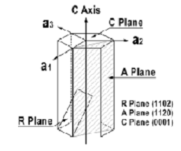
Orientation
1. Orientations
Sapphire 는 Hexagon/rhombohedral 구조로 많은 특성이 결정의 방향에 따라 결정이 된다. Epi growth 에 대해서는, 다른 결정 방향은 epi 물질과 일치하는 격자상수의 범위를 가져야 한다.
2. Substrates
C-plane sapphire 기판은 Blue LED 에 사용되는 GaN 과 같은 3-5족과 2-4족에 사용되어진다. 더욱이, C-plane 은 infrared detector 의 적용분유에 유용하다.
A-plane 기판은 일정한 유전율을 가지고, hybrid microelectronic application 에 사용되어지는 높은 절연성을 또한 가진다. High Tc superconductors 은 이 기판을 사용하여서 만들어질 수가 있다.
R-plane 기판은 microelectronic IC 에 사용을 위해서 실리콘의 Hetero-epitaxial 증착에 사용되어진다. Sapphire 는 높은 유전율 때문에 microwave IC 와 같은 hybrid 기판에 사용이 적당하다. 게다가, epitaxial 실리콘 과정에 필름을 바를 때, 빠른 속도의 IC 와 pressure transducers 이 만들어 질 수 있다. Thallium 성장시, 다른 superconducting components, high impedance resistors, and GaAs 이 적용될 수 있다.
3. Application
- GaN, 3-5 족, 2-4족 Compounds
- IR Detectors
- High Tesuperconductors and High Frequency Dielectrics.
High speed IC's and Pressure Transducers
GaAs wafer carriers
SOS (Silicon On Sapphire)
Orientation : A-Plane(1120), C-Plane(0001), R-Plane(1012) 또는 Size up to 4" diameter. |

|
당사에서는 Polished Sapphire Wafer에 대해서 다음의 Spec이 공급 가능합니다.
Specification of polished Sapphire Wafer
Type: polished Monocrystalline, SEMI M3-91
Material: Kyropolos high-purity monocrystalline AI2O3
Orientation: C-, A-, R- Plane ± 0.25 degree, ± 0.10 degree on request
Diameter: 2 inch - 6 inch ± 0.50 mm, C-Plane: 2 inch - 5 inch
Physical parameters:
Thickness, Center Point: SEMI or on request > 0.25 mm
Toatal Thickness Varaiation TTV: < 10 microns; typical, other on request
Bow: < 15 microns; typical for 2 inch
Taper: < 15 microns; typical for 2 inch
Primary Flat: SEMI standard, or on request
Orientation: according to SEMI standard ± 0.5 deg.
Front surface finish:
Particles: < 10 @ 0.3 microns
Roughness (Ra): < 1.0 nm; typical, others on request
Surface quality: Epitaxial polishing (MIL 20-10)
Back surface:
Surface quality: Fine grinding
Package: 25 wafers, EMPAK Ultrapack cassette, double bagged
Specification of Ground Sapphire Wafer
Type: Ground finish
Material: Kyropolos high-purity monocrystalline AI2O3
Orientation: C-, A-, R- Plane ± 0.25 degree, ± 0.10 degree on request
Diameter: 2 inch - 6 inch ± 0.50 mm, C-Plane: 2 inch - 5 inch
Physical parameters:
Thickness, Center Point: SEMI or on request > 0.15 mm
Toatal Thickness Varaiation TTV: < 20 microns; typical, other on request
Bow: < 20 microns; typical for 2 inch
Taper: < 20 microns; typical for 2 inch
Primary Flat: SEMI standard, or on request
Orientation: according to SEMI standard ± 0.5 deg.
Front surface finish:
Roughness (Ra): 0.8 - 1.2 microns
Surface quality: ground, ready for polish
Back surface:
Roughness (Ra): 0.8 - 1.2 microns
Surface quality: ground, ready for polish
Package: to prevent breakage |
|
|


|
|

|
| 홈페이지 |
: |
http://daihanscience.koreasme.com |
| 회사명 |
: |
http://www.daihan.net 대한과학연구기자재 |
| 전화번호 |
: |
(1)02-967-5978 비상연락 (H.P) : 011-768-8228
(2)02-3673-0199
|
| 팩스번호 |
: |
(1)02-967-5979
(2)02-3673-0271
|
| 주소 |
: |
(1)서울특별시 성북구 상월곡동 24-4 대한빌딩서울 (우편번호: 110-123)
(2)서울 종로구 인의동 웅진빌딩 별관 210호 (우편번호: 110-785)
(3)■ 택배/화물서비스 : 당사에서는 100,000원 이상 구매 고객 분 에게는 당사에서 부담합니다 ( 택배 : KGB, 삼성, 화물 : 양양,대신,호남) ........................... 주거래은행 : ■ 예 금 주 : 김 민 옥■ 우리은행 : 048 - 401225 - 13 - 001 ■ 기업은행 : 086 - 023287 - 03 - 019 ■ 국민은행 : 045 - 24 - 0267 - 056
|
| URL |
: |
(1)http://www.daihan.net
(2)http://대한과학.net
|
| E-mail |
: |
daihansci@yahoo.co.kr |
|
|
|


